Presentation will begin: Wednesday, October 21, 2026 - 10:35 AM
Semiconductor Inspection Using Infrared Microscopy: From Alignment to Stress Analysis
Presented by:
Helene-Sarah Becotte, Jay PhotonicsAs semiconductor devices evolve toward increasingly complex 3D architectures, inspection challenges extend well beyond the surface. Engineers must visualize buried structures, verify multilayer alignment, and identify stress or defects without compromising the sample or disrupting manufacturing workflows. While existing inspection techniques each provide valuable information, they often require trade-offs in resolution, throughput, sample preparation, or system complexity.
This presentation introduces an advanced infrared transmission microscopy approach designed to bridge the gap between conventional optical inspection and more complex analytical techniques. Combining high-resolution subsurface imaging with compatibility across existing microscope platforms, the technology enables direct visualization of buried semiconductor features in real time. Through practical examples, we will explore how this approach supports two key inspection applications: alignment verification in multilayer devices and wide-field stress analysis, revealing information that can be difficult to obtain using conventional optical methods alone.
Attendees will gain a practical understanding of where advanced infrared transmission microscopy fits within today's semiconductor inspection toolbox, the inspection challenges it is designed to address, and how it complements existing techniques for process development, failure analysis, and manufacturing.
About the presenter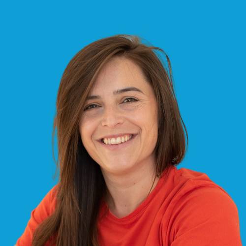
Helene-Sarah Becotte, Ph.D., is the CEO and co-founder of Jay Photonics, where she leads the commercialization of infrared microscopy solutions for semiconductor inspection. She works closely with industrial and academic partners to translate advanced imaging technologies into practical tools for semiconductor R&D, failure analysis, and manufacturing.
She holds a doctorate in applied mathematics from Polytechnique Montréal. Before cofounding Jay Photonics, she founded and led her own consulting business, specializing in mathematical modeling and decision-making. Her background combines entrepreneurship, applied mathematics, and technology commercialization, bringing a practical perspective to the adoption of emerging photonics technologies.